Cleanroom-Grade Silicone Keypads for Wafer Probers and Final Testers – Why "Just Any Keypad" Won't Cut It
- Share
- publisher
- Suey
- Issue Time
- Aug 17,2026
Summary
Cleanroom-grade silicone keypads are critical for wafer probers and final testers to eliminate contamination, ESD failures, and contact drift. Standard alternatives cause yield loss and downtime. FromRubber delivers custom, precision-engineered keypads with anti-static coatings and low-outgassing for reliable semiconductor testing.
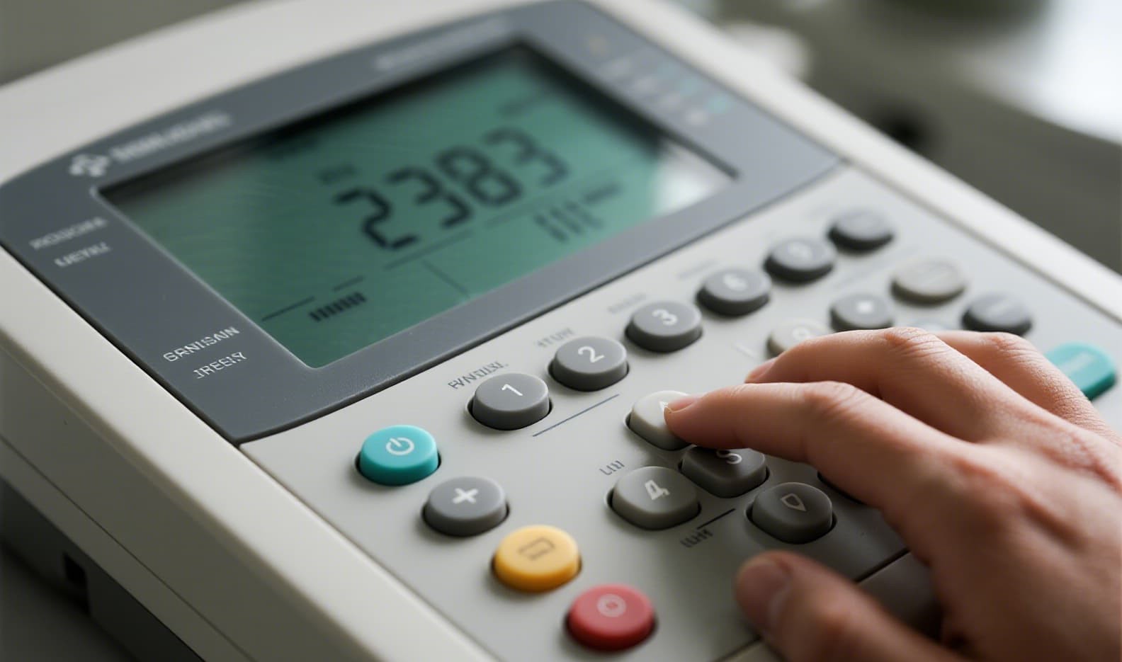
In semiconductor manufacturing, the wafer prober and final tester are where chip meets reality. Every touchdown of a probe card, every parametric measurement, and every functional test depends on equipment that must perform with absolute precision in environments where one stray particle or one millisecond of signal noise can ruin an entire lot. The human-machine interface — the silicone keypads that operators use to control these systems — is often overlooked. But when that keypad fails, the entire test floor stops.
This isn't about aesthetics. It's about yield, uptime, and the integrity of semiconductor test data. Here's why cleanroom-grade silicone keypads are non-negotiable for wafer probers and final testers — and why "just any keypad" will cost you far more than its purchase price.
1. The Cleanroom Imperative: Silicone Keypads Particles Are the Enemy
Wafer probing and final test occur in ISO Class 5 to Class 7 cleanrooms (formerly Class 100 to Class 10,000), where airborne particle counts are strictly regulated. A standard silicone keypad molded in a non-cleanroom environment can shed particles — microscopic silicone fragments, dust from tooling, or contaminants embedded during secondary operations like printing or coating.
Once those particles settle on a wafer surface or probe card, they become killer defects. They can scratch probe needles, create electrical leakage paths, or interfere with the optical alignment systems used in advanced probers. In extreme cases, outgassing from improperly cured silicone can deposit volatile organic compounds onto wafer surfaces, directly impacting yield.
2. ESD Protection: Not Optional, It's Critical
Standard silicone rubber is an electrical insulator with surface resistivity exceeding 10¹² Ω/sq. In a wafer prober or tester environment, that's a problem. Every actuation of a keypad can generate triboelectric charge. If that charge discharges through a sensitive device under test (DUT), it can cause latent or catastrophic ESD damage — failures that may not manifest until final system integration.
Cleanroom-grade keypads for semiconductor test equipment incorporate anti-static or conductive treatments to drain static charges safely. This can be achieved through:
- Anti-static coatings (surface resistivity 10⁵ – 10⁹ Ω/sq) — dissipates charges slowly, ideal for ESD-safe cleanroom use.
- Bulk conductive silicone (<10³ Ω/sq) — permanent conductivity, unaffected by wear, suitable for high-reliability test interfaces.
At FromRubber, every cleanroom-grade keypad destined for semiconductor applications is evaluated for ESD performance. We apply coatings selectively — only where needed — to preserve the soft-touch feel of silicone while ensuring that the keypad never becomes a static source.
3. Electrical Conductivity of Silicone Keypads: Contact Resistance That Stays Stable
A wafer prober or final tester may cycle through thousands of devices per shift. The keypad's conductive carbon pills or contact domes must deliver consistent, low-resistance switching for the life of the equipment. Typical requirements call for contact resistance below 100 Ω, with actuation forces in the 125–150 gf range and snap ratios of 40–60% for optimal tactile feedback.
When a keypad is manufactured with inconsistent carbon pill geometry or poor adhesion between the conductive pad and the silicone substrate, contact resistance drifts. Operators press harder. The tactile feel degrades. And eventually, the key fails to register — or worse, registers intermittently, creating false test results.
FromRubber addresses this through precision molding in Class 1000 cleanrooms, achieving dimensional tolerances of ±0.05 mm. Every keypad undergoes 100% final inspection, including actuation force verification (within ±15 g of specification) and continuity testing with custom fixtures.
4. Two Case Studies: When Precision Matters Most
Case Study 1: Silicone Keypads for Wafer Probers Retrofit — Particle Contamination Eliminated
A major semiconductor equipment manufacturer was experiencing intermittent probe card contamination on their 300 mm wafer probers. After extensive troubleshooting, they traced the source to the silicone keypads on the operator control panel. The keypads — sourced from a general-purpose supplier — were shedding microscopic silicone particles that migrated into the probe card area.
FromRubber replaced the keypads with cleanroom-molded, post-cured silicone keypads manufactured in an ISO Class 7 environment. The new keypads incorporated a low-outgassing formulation and anti-static coating. Result: probe card contamination incidents dropped by 94%, and mean time between cleanings extended from weekly to quarterly.
Case Study 2: Silicone Keypads for Final Testers — ESD Failures Resolved
A semiconductor test house running high-volume final test for automotive microcontrollers was seeing an unexplained 2.3% ESD failure rate. The failures were intermittent and occurred after operator interactions with the test system's keypad interface.
Investigation revealed that the standard silicone keypads were generating triboelectric charges during normal operation. FromRubber engineered a replacement keypad with bulk conductive silicone (surface resistivity < 10³ Ω/sq) and a redesigned grounding path. The new keypads also featured enhanced tactile geometry with a snap ratio optimized for gloved-hand operation. ESD-related failures dropped to below 0.1% — and operator fatigue decreased significantly thanks to the improved tactile response.
5. Durability That Matches Your Equipment Lifecycle
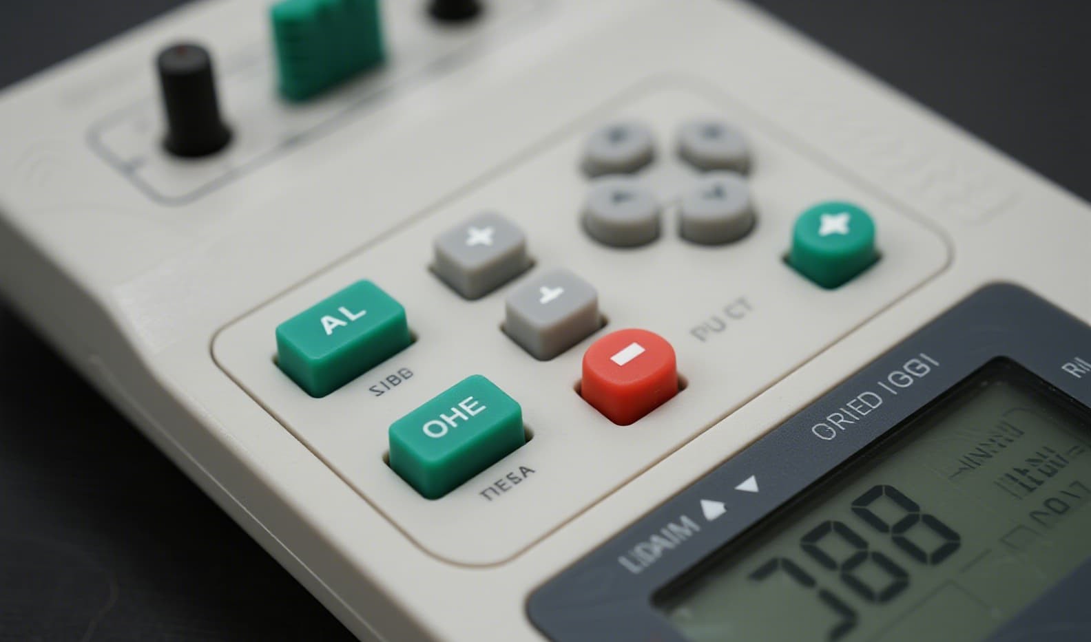
Wafer probers and final testers are capital equipment designed for decades of service. The keypad should not be the weakest link. Cleanroom-grade keypads from a specialized manufacturer are engineered for 1 million+ actuations without tactile degradation. They withstand temperature cycling from -40°C to +125°C and resist chemical exposure from routine cleaning solvents.
FromRubber's keypads are tested to IEC 61058-1 actuation life standards and undergo environmental aging at 85°C / 85% RH for 500 hours with no delamination or resistance drift. That's the kind of reliability that keeps test floors running.
6. Why Choose FromRubber?
With over 15 years of experience in custom silicone keypad engineering, FromRubber is not just a component supplier — we are a strategic partner for semiconductor equipment manufacturers. We specialize in:
- Cleanroom molding — ISO Class 7 (Class 1000) with full in-house process control.
- ESD-safe materials — anti-static coatings and bulk conductive compounds tailored to your requirements.
- Precision engineering — ±0.05 mm dimensional tolerances and 100% final inspection.
- End-to-end service — from DFM analysis and prototyping to mass production and just-in-time delivery.
We don't believe in "one size fits all." Every wafer prober and final tester has unique interface requirements — different key layouts, specific force-travel curves, integration with backlighting or EMI shielding. FromRubber works with your engineering team to design, validate, and deliver keypads that perform flawlessly in your specific test environment.
7. The Bottom Line
"Just any keypad" might save you a few dollars on the BOM. But in a semiconductor test environment, that saving is an illusion. Particle contamination, ESD failures, contact drift, and premature wear all translate to lost yield, unscheduled downtime, and scraped wafers. The true cost of a substandard keypad is measured in thousands — or millions — of dollars of lost production.
Cleanroom-grade silicone keypads from a specialized manufacturer are not an expense. They are an investment in equipment reliability, test data integrity, and operational uptime.