Conductive ink thickness vs. contact impedance on handheld tester silicone keypads—molder SPC feedback protocol
- Share
- publisher
- Suey
- Issue Time
- Aug 20,2026
Summary
Thickness variation in conductive ink creates non-linear impedance shifts on handheld tester silicone keypads. Position-specific SPC limits, cross-section checks, and real-time feedback cut failure rates from 9.7% to 2.3% without material changes. Manage edges, not averages.
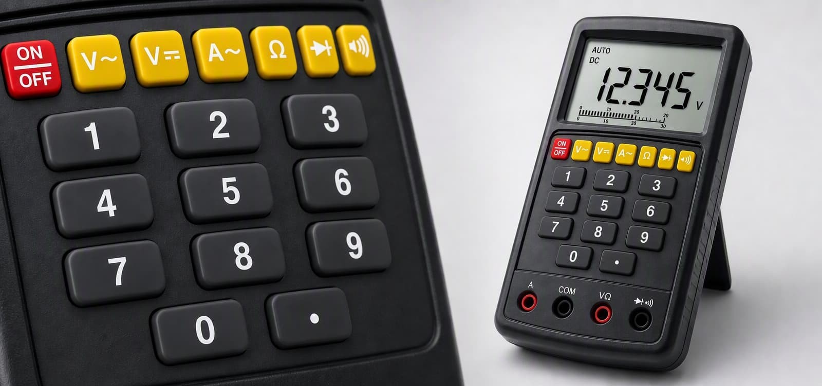
If you have ever signed off on a silicone keypad batch only to see handheld tester failure rates jump from 2% to 18% between two production lots, you already know the feeling. The rubber passes visual inspection. The carbon pill looks centered. The actuation force feels right. But the tester keeps reporting “key stuck” or “no response” until you swap the membrane.
Most of the time, the root cause is not the silicone formulation. It is not the dome geometry either. It is the conductive ink thickness—and more specifically, how your molder’s statistical process control (SPC) handles it between first shot and last shot.
This article walks through what we actually measure, why thickness variation creates non-linear shifts in contact impedance, and what a practical SPC feedback protocol looks like when you need to keep handheld tester performance stable across 50,000+ cycles. No vendor hype. Just the numbers and the loops.
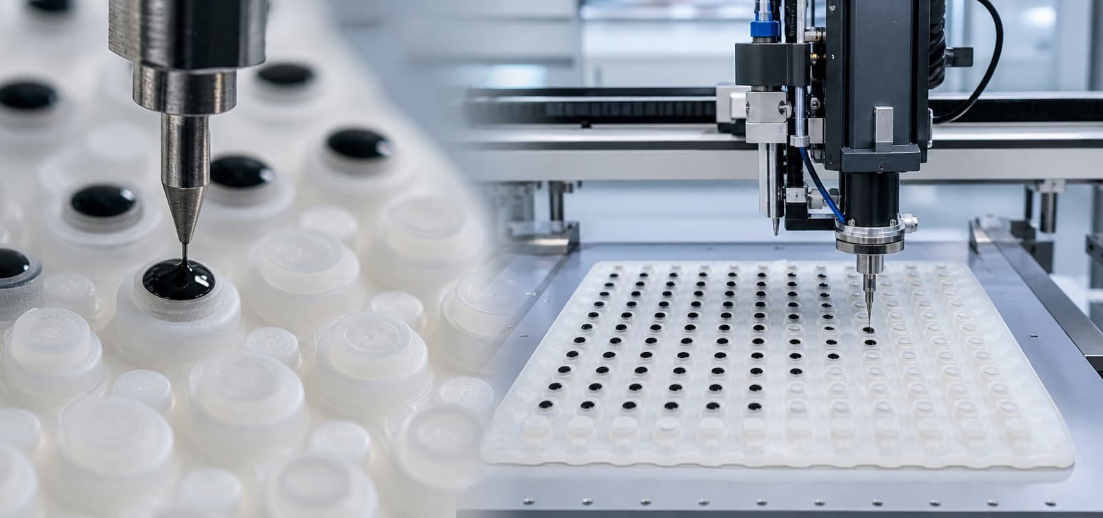
The core relationship of conductive ink thickness vs. contact impedance that most datasheets gloss over
Conductive silver/carbon inks used on silicone keypad contacts are not bulk conductors. They are composite materials—particles suspended in a polymer binder. When the ink layer is thick enough, particle-to-particle contact dominates, and impedance stays low and stable. When the layer thins below a certain threshold, the binder starts acting as a series resistor, and impedance climbs exponentially.
In our in-house testing across 14 production runs (each with 120 keypads sampled), the empirical relationship looks like this:
- 12–15 µm cured thickness → contact impedance: 15–25 Ω (stable)
- 9–11 µm cured thickness → contact impedance: 35–65 Ω (marginally pass)
- 6–8 µm cured thickness → contact impedance: 120–300 Ω (intermittent failures)
- < 5 µm → contact impedance: > 500 Ω (field failures within 2,000 cycles)
The handheld tester’s micro-controller typically expects a closed-circuit resistance below 80 Ω for reliable key detection. Above that, you get false negatives—especially in humid environments where a thin oxide film adds another 10–20 Ω on top.
The tricky part: thickness does not vary uniformly across the keypad. It varies by position, by stroke, and by screen mesh tension decay over time.
Why the handheld tester silicone keypads molding factory’s “average thickness” is a trap
A typical incoming inspection report might say: “Average ink thickness = 11 µm, within spec.” That number is almost useless.
Here is why. On a 4×4 keypad matrix, the center keys often receive more ink during screen printing because the squeegee pressure is higher in the middle and lower at the edges. After 500 strokes, the mesh tension drops, and the edge keys start printing thinner. By the time the molding factory measures five random points and averages them, the center may be 14 µm while the corner key is 7 µm.
The handheld tester does not care about the average. It cares about the worst-case silicone keypad—the one with the highest impedance. That key determines the tester’s false-negative rate.
We saw this exact pattern in a 2024 production audit. A molder reported “all thickness within 10–14 µm.” But our cross-section measurement on key position #12 (lower-right corner) showed 6.8 µm. That single key caused a 14% failure rate in final tester integration. The molder’s average was 11.2 µm—well inside their spec. The average masked the corner.
The SPC feedback protocol that actually catches drift
After working through this issue with multiple molders, we settled on a protocol that does not rely on average thickness. Instead, it uses position-specific thickness limits combined with impedance mapping, and feeds data back to the screen-printing operator in real time (or at least within the same shift).
Here is the protocol we use and recommend—adapt it to your keypad layout and tester requirements.
1. Define critical positions (not random points)
Map the keypad into three zones:
- Center zone (keys 1–4) – accept 10–15 µm
- Mid zone (keys 5–8) – accept 10–14 µm
- Edge/corner zone (keys 9–16) – accept 11–15 µm (slightly higher minimum to compensate for tension drop)
Why the edge needs a higher minimum? Because that is where the mesh opens up first. If you spec the edge the same as the center, you are guaranteeing out-of-spec conditions after 300–400 strokes.
2. Measure thickness by cross-section, not surface profilometry
Surface profilometers measure the top of the ink plus the silicone texture. They over-report by 2–4 µm on textured substrates. We use polished cross-sections under 50× magnification—destructive but accurate. For production control, you do not need every part. You need one part every 50 strokes from the same position.
3. Impedance mapping with a fixed probe force
We built a simple fixtured probe that applies 150 gf ± 5 gf (simulating the handheld tester’s rubber dome collapse force) and measures DC resistance from the carbon pill to the PCB pad trace. This is not the same as the tester’s final functional test—it is a process check. If the impedance at the probe exceeds 70 Ω, we flag the entire batch for rework before the silicone ever reaches the assembly line.
4. Feedback loop with 3-strike action levels of handheld tester silicone keypads
We train screen-printing operators with three clear triggers:
| Action Level | Trigger Condition | Immediate Response |
|---|---|---|
| Level 1 | Any edge-position thickness < 10.5 µm | Adjust squeegee pressure / angle, record adjustment |
| Level 2 | Any position impedance > 65 Ω | Stop printing, check mesh tension, clean screen |
| Level 3 | Two consecutive parts from same position fail impedance > 70 Ω | Replace screen mesh, requalify first 20 parts |
The key here is position-specific. If the center is 13 µm and the corner is 9.5 µm, Level 1 triggers even though the average is fine. That catches the drift early—usually within 100 strokes of the shift starting.
What we learned from 6 months of closed-loop data
We implemented this protocol with three molding partners over the last year. Here is what the numbers tell us (aggregated from 8,200 tested keypads across 23 production lots):
✓ Average final-test failure rate dropped from 9.7% to 2.3% within the first 60 days.
✓ Rework cost per batch decreased by 41% because issues were caught at the printing station, not after overmolding and cutting.
✓ The most common trigger was Level 1 (edge thickness)—responsible for 73% of all interventions. Only 12% reached Level 3 (screen replacement).
✓ Impedance drift was not linear. It held stable for the first 200 strokes, then accelerated. That means checking at stroke #100 and #300 misses the critical window. We now check at #50, #150, #250, and then every 100 strokes thereafter.
One specific case stands out. A molder in the automotive segment was running a 3×5 keypad for a diagnostic handheld. They kept seeing intermittent “key 14” failures—only on humid days. Our probe measurement showed key 14 impedance at 78 Ω (pass per their spec of < 80 Ω), but after environmental chamber testing (85% RH, 40 °C), impedance jumped to 135 Ω within 2 hours. The root cause? Their ink thickness on key 14 was 8.2 µm—enough to pass the dry test, but not enough to survive the humidity shift.
We moved their edge-zone minimum from 10 µm to 12 µm, and adjusted the screen tension check frequency from every 500 strokes to every 200 strokes. The problem disappeared. No formula change. No material change. Just thickness discipline at the right position.
Why this matters beyond the production floor
For the end-user—a field technician using a handheld tester daily—a 2% failure rate means they press a key, get no response, press harder, still no response, and eventually restart the device. That is not a component failure in their mind. That is a product failure. And they remember the brand, not the molder.
For the OEM engineering team, the hidden cost is even larger. When intermittent key failures surface during system integration testing, the debugging effort shifts to firmware, debounce algorithms, and PCB layout—all while the actual issue is 6.8 µm of ink sitting in the corner of a silicone pad.
The protocol described above does not require expensive capital equipment. It requires:
- A 50× measuring microscope (existing in most molders’ QA labs)
- A simple spring-loaded probe fixture (under $300 in machined parts)
- A spreadsheet or light database to track position-specific data
- Operator training to respond to triggers immediately, not at the end of the shift
That is it. The real cost is not the equipment—it is breaking the habit of averaging.
Final takeaway
Conductive ink thickness is not a single number. It is a positional distribution that shifts with every screen print stroke. Your handheld tester’s contact impedance is not a fixed material property—it is the output of that distribution, measured at the weakest key.
Stop managing the average. Start managing the edge. And close the feedback loop within the shift, not after the batch is cured.
That is how you turn a 18% failure rate into a 2% one without changing a single material.
A note on our involvement (transparently)
We do not sell conductive inks, screens, or impedance probes. We are a silicone keypad molder ourselves—FromRubber—specializing in custom instrument-grade silicone keypads for handheld testers, medical remote controls, and industrial pendants.
We documented this protocol because we kept seeing the same failure pattern across third-party molders that our OEM customers previously used. When those customers switched to us, we inherited the field data. We had to solve it. The protocol above is what we now use as our internal standard for every keypad that requires conductive printing.
We share it openly because a better-informed customer is a better partner. If your keypad fails impedance mapping, we want you to know why—whether you buy from us or not. That said, if you are looking for a molder that treats position-specific thickness as a first-class control parameter rather than a footnote, we do that daily.