Digital Inclinometer Silicone Keypad Integration Problems in Compact Instrument Enclosures
- Share
- publisher
- FromRubber
- Issue Time
- Sep 16,2026
Summary
Compact digital inclinometers leave very little room for a keypad, and the problems that appear during assembly are dimensional rather than electrical. This article covers keypad-to-enclosure fit, button position against PCB contacts, thickness and compression space, locating features, material hardness, and the prototype checks worth running before tooling.
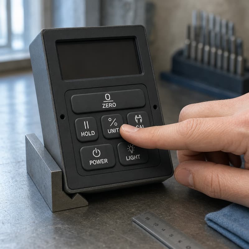
The first samples of a compact digital inclinometer usually work. The problems start at tooling review, when someone notices that the housing no longer closes without force. Nothing about the electronics changed. What changed is that the keypad, the PCB and the enclosure were all designed to fit, and none of them was designed to fit together. A handheld digital inclinometer is one of the harder instrument formats to put a keypad into. The housing is small, the display takes most of the front face, and the buttons have to sit in whatever area is left. That leftover area is usually narrow, irregular, and shared with the seam between the front and rear housing halves. Several constraints arrive at the same time: The practical consequence is that a digital inclinometer silicone keypad cannot be treated as an isolated part. It has to be dimensioned against the PCB, the plastic housing, the display window, the internal support structure and the button openings at the same time, using one reference system. Integration decisions belong in the mechanical design phase, not in a supplier's inbox. Once the housing steel is cut, the only remaining variables are the keypad and the board position, and those two cannot absorb every error on their own. Most of the problems we see during development fall into three families. They are worth treating separately because each is fixed by a different drawing. The keypad outline is the first dimension anyone checks, and it is often the wrong one to check first. What matters is not the overall size on the drawing but the fit against the features that actually locate the keypad. When the dimensional assumptions are not shared, the keypad arrives slightly too large and the assembly team compresses it. Silicone tolerates that once. It does not tolerate it as a production routine, because the compression is transferred into the buttons, and a pre-loaded button does not reset reliably. Fit clearance design has its own logic, and we set out the numbers and the failure patterns in the guide to silicone keypad and plastic enclosure fit clearance. The second family of problems is positional. Four elements have to agree: the silicone button plunger, the conductive carbon contact on the plunger, the PCB switch pad, and the opening in the plastic housing. They are produced by three processes, and a deviation in any one of them changes the switching behaviour. The reason small deviations matter so much is the shape of the response. A conductive contact landing 0.1 mm off centre on a 3 mm pad barely changes anything. The same offset on a 1.2 mm pad removes a meaningful part of the contact area, and the button becomes sensitive to how it is pressed rather than to whether it is pressed. The third family is vertical. In a compact housing, thickness is where tolerance goes to hide, and it accumulates quietly: The compression area has to be defined at the mechanical design stage. Retrofitting compression space after the housing is moulded means either a taller button, a thinner keypad, or a spacer — and a spacer in a handheld instrument costs volume that the design does not have. A custom silicone keypad is not a flat sheet with bumps on it. It is a moulded structure, and the way that structure is organised determines whether it assembles reliably in a tight housing. The keypad in the photograph illustrates a common compromise. The button field is not a simple rectangle: the upper row is wider than the lower row, the outline is asymmetric, and two fixing holes sit outside the button area. That shape follows the available front-face area after the display and the housing seam have taken their share. The base web sets the personality of the whole panel: The base has to be flexible without being loose. A base that is too flexible lets the whole panel shift when one button is pressed, which transfers force into neighbouring buttons. A base that is too stiff raises the actuation force for every button on the panel, which is a difficult problem to solve later because it is set by the mould. Plunger height is the dimension that links the keypad to the board. It has to be matched to the PCB contact location, and it interacts with four other numbers: When these are not checked together, the visible symptom is usually a button that feels fine in the open assembly and different once the housing is screwed shut — because closing the housing changed the compression distance. Locating holes, pins, grooves and moulded steps do one job: they remove the operator from the positioning decision. In a compact instrument, where the keypad may be placed into the housing before the board is fitted, this matters more than it does in a large panel. A locating feature converts a judgement into a fit: the keypad either settles onto its post or it does not. This is the part of the project where a few hours of drawing review saves weeks of sampling. Alignment depends on the relationship between five sets of features: Each of these has a tolerance. Each tolerance has a direction. When all five are referenced from the same mechanical datum system, their contributions can be added and compared against the available button travel. When they are referenced from whatever was convenient for each party, the sum is unknown, and the assembly becomes a coin toss that a prototype run of ten units will not reveal. A keypad manufacturer does not design the instrument's board. What a keypad manufacturer needs is accurate contact information from the board that already exists. The exchange is straightforward and should include: Two-way drawing exchange is what makes a custom keypad quotation meaningful. A quotation based on a hand sketch and an approximate button count is a placeholder, not a schedule. The DFM questions worth asking before tooling are collected in our note on DFM rules for silicone keypad and enclosure integrated design. Tolerance stack-up is easier to understand with a physical picture than with statistics. Imagine laying five thin plates on top of each other. Each plate is within its own specification. If every plate happens to be at the thick end, the stack is visibly taller than the drawing suggests, even though nothing is out of tolerance. In an inclinometer keypad assembly, the plates are: Button switching is not a gradual function of dimension. It is close to a step: either the contact closes or it does not. That is why a 0.15 mm error, which is invisible on a housing drawing, can produce a hard functional fault. Experienced development teams treat the small dimensional deviations in this list as design inputs rather than as production noise. The alternative — tightening every tolerance on the drawing — raises cost on features that do not matter and leaves the features that do matter unchanged. We wrote about that trade-off in over-specified keypad tolerances and tooling cost. In a small instrument, material choice is felt rather than measured. The same geometry in a softer compound feels comfortable but may not reset reliably; in a harder compound it resets cleanly but the small buttons on a narrow panel become tiring to use. Standardised hardness measurement exists for a reason, and stating a silicone hardness on a drawing is only useful if both parties measure it the same way. ASTM D2240 describes the durometer method and the instrument types used for elastomers, and it is the reference we work to when a customer specifies a hardness figure. Material selection should follow the instrument's operating environment and expected button usage. A hardness chosen solely because it feels good in the sample room tends to disappoint in a cold workshop or in a housing that has been sitting in a van. Some integration decisions are worth making deliberately, because they remove failure modes without adding parts. The keypad below shows a denser layout than the previous example: eight functions on a small panel, with ZERO, HOLD and UNIT in the upper block and the frequently used measurement keys grouped beneath. Two locating holes sit at the mid-height of the panel, where they also act as a visible check that the keypad is seated the right way round. Even spacing is not only about appearance. It keeps the web between buttons uniform, so each button has a similar amount of material separating it from its neighbour. When one gap is reduced to make room for a display window, that button deflects differently from the rest, and the panel develops a feel anomaly that is very hard to correct after tooling. Travel has to be matched to what the PCB switch needs to activate, and then checked again with the housing closed. In a compact instrument, travel is usually limited by the housing opening depth rather than by the silicone. That makes travel a shared responsibility: the keypad sets the available stroke, and the housing sets the mechanical stop. Moulded locating features improve repeatability with no extra component cost, because they are formed in the same operation as the keypad itself. The main requirement is that the feature and the housing that receives it are dimensioned from the same datum. A locating hole that is accurate to its own drawing but referenced differently from the housing post provides no benefit at all. The base has to balance flexibility with dimensional stability. In a compact housing with a narrow panel, that balance shifts towards stability, because the panel has less room to absorb deflection. Web thickness, button wall thickness and material hardness are the three levers, and they trade against each other rather than acting independently. Prototype validation is not a formality in compact instruments, because the errors being tested for are exactly the ones that only appear when the housing is closed. A sample keypad held against a bare board will tell you almost nothing about whether the finished instrument will work. Prototype testing is cheapest when it happens before tooling and most valuable when it reproduces the closed assembly. Testing a keypad in isolation confirms the keypad; testing it in the housing confirms the design. The quality of a custom keypad quotation depends almost entirely on the technical package behind it. These are the items we ask for before quoting, and the ones that most often arrive late: Complete information does two things at once. It improves design accuracy, and it reduces revisions, because the assumptions that would otherwise be made silently are made explicitly instead. In our experience the projects that go smoothly are not the ones with the simplest geometry; they are the ones where the drawing package arrived complete before anyone cut steel. Successful integration of a digital inclinometer silicone keypad comes down to design coordination between four things: the keypad structure, the PCB layout, the enclosure dimensions and the assembly sequence. None of them is difficult on its own. The difficulty is that they belong to different drawings and often to different organisations. Early technical communication between the instrument manufacturer and the keypad supplier is what makes the difference. Dimensional and functional problems are almost always visible on paper before they are visible in a housing, and the cost of a drawing revision is a fraction of the cost of new tooling or a field failure. If you are working on a compact instrument and have housing and board drawings available, we can review the keypad interface dimensions against them and tell you where the stack has no margin left. FromRubber manufactures custom silicone keypads and buttons to customer drawings; we do not design PCBs or instrument housings, which is exactly why we ask for both before quoting. FromRubber is the trading name of Dongguan Bohao Electronic Technology Co., Ltd., a custom silicone keypad manufacturer producing compression-moulded and LSR silicone keypads, buttons and seals to customer drawings. The figures discussed here are engineering orientation for interface design, not a specification for any particular instrument.Why Digital Inclinometer Silicone Keypad Integration Requires Careful Design
Where integration work belongs
Common Integration Problems with Digital Inclinometer Silicone Keypads
Keypad Dimensions Do Not Match the Enclosure
Button Positions Do Not Align with the PCB Contacts
Keypad Thickness Creates Assembly Interference
How Silicone Keypad Structure Affects Compact Instrument Assembly
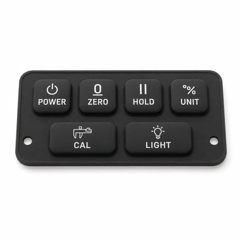
Keypad Base and Supporting Web Structure
Button Plunger Height and Contact Position
Locating Features and Anti-Misalignment Design
PCB and Silicone Keypad Alignment Considerations
Using PCB Drawings as a Reference for Keypad Development
Tolerance Stack-Up in Digital Inclinometer Silicone Keypad Assemblies
Why Small Dimensional Deviations Can Cause Large Functional Problems
Observed symptom
Typical dimensional contribution
Button cannot fully press the PCB contact
Plunger height short, or board sitting high in the stack
Button remains partially compressed after release
Housing pre-load, or base web too thick for the available space
Adjacent buttons interfere with each other
Supporting web too heavy, or button spacing reduced without reducing web stiffness
Housing assembly creates excessive pressure
Keypad outline at the high limit against housing cavity at the low limit
Uneven tactile feedback between buttons
Housing wall warp, or non-uniform ledge contact across the panel
Material and Hardness Considerations for Compact Digital Instruments
Design Features That Improve Digital Inclinometer Silicone Keypad Integration
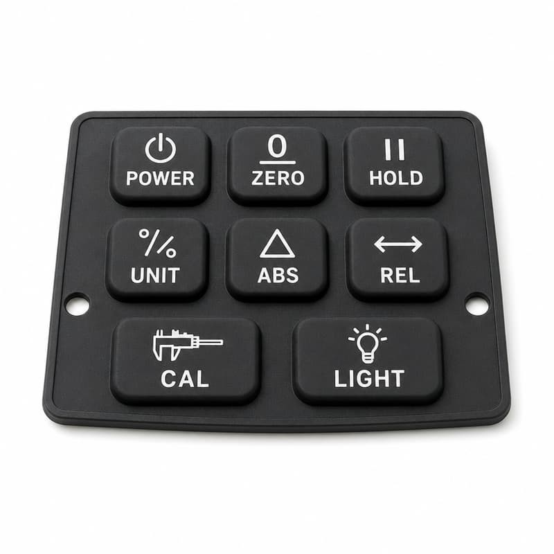
Consistent Button Spacing
Controlled Button Travel
Integrated Locating Structures
Flexible but Stable Silicone Base
Prototyping and Testing Before Mass Production
Information Required for Custom Digital Inclinometer Silicone Keypad Development
Practical Checklist for Digital Inclinometer Silicone Keypad Integration
Conclusion
References and Standards Cited
Related reading