Electronic Level Silicone Keypad Button Alignment Problems During PCB Assembly
- Share
- publisher
- FromRubber
- Issue Time
- Sep 16,2026
Summary
Button alignment between a silicone keypad and a PCB is usually decided long before assembly. This article works through the causes of misalignment in electronic level keypads, how plunger and contact geometry interact, which PCB and housing drawings a keypad maker needs, how tolerance stack-up behaves across three moulded parts, and the assembly checks that catch a mismatch while it is still cheap to fix.
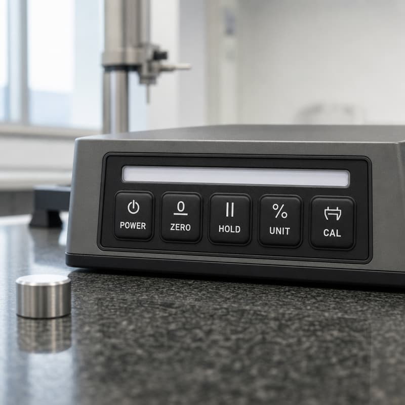
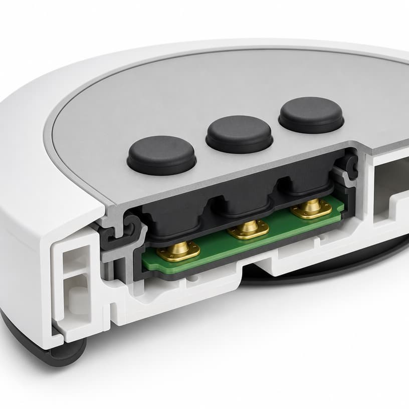
A level that zeroes cleanly on the bench and then refuses to zero on site is rarely an electronics problem. More often, one button on the keypad is pressing its PCB pad slightly off centre. It still switches — for a while. Then it needs a firmer thumb, then two presses, then a service visit. By the time anyone opens the housing, the tooling has been paid for and the fix is no longer a drawing change. An electronic level is a measuring instrument, so a button that fires late is more than an inconvenience. An operator rests the unit on a machined surface with one hand and presses ZERO or HOLD with the other, usually wearing gloves and usually not looking closely at the display. That habit puts each button in a fixed relationship with three other parts at the same time: the silicone keypad moulding, the PCB underneath it, and the housing that clamps the stack together. If those three are dimensioned from different reference points, the assembly still closes. The error simply hides inside the button travel, where nobody measures it. What a misaligned electronic level silicone keypad looks like on the line is fairly consistent: Alignment is not one dimension. It is the agreement between the button centre on the PCB drawing, the plunger centre in the keypad mould, and the centre of the opening in the housing. Two of the three can be perfect and the third can still ruin the assembly. In practice, misalignment rarely comes from a single blunder. It comes from three small, individually reasonable decisions that stack up. The pattern repeats often enough that it is worth separating the causes before discussing cures. The PCB contact pad centres and the silicone plunger centres have to agree. They are produced by two different parties from two different drawings, and the exchange between them is where most errors enter the project. Carbon pill and conductive contact placement inside the keypad is covered in more detail in our note on conductive pill misalignment and locating hole design. A PCB is not pinned in space. It is located by screws, posts, or a moulded ledge, and each of those has its own clearance. A board held by four M2 screws through 2.4 mm holes can shift position by a surprising amount before the screws are tightened. Escape clearance and support geometry are treated separately in our article on avoiding PCB interference through escape clearance design. Tooling is only as accurate as the drawing it was cut from, and it is cut once. If the keypad mould is based on an unconfirmed revision, the error is fixed in steel. Silicone shrinkage compounds the problem: the mould cavity has to be scaled to compensate, and that compensation is calculated per material and per wall thickness, not applied as a universal factor. Two practical consequences follow. First, no keypad mould should be cut until the PCB drawing is under revision control. Second, the first samples have to be measured against the same datum system the PCB uses, not simply eyeballed in the housing. The switching path in a silicone keypad is short and entirely mechanical. A silicone button cap is connected to a plunger. The plunger carries a conductive carbon pill, or it pushes against a metal dome. Underneath sits the PCB contact pad. Four elements, three of which are made by the keypad supplier and one by the instrument maker. Because the whole path is mechanical, alignment has to be read in two directions at once. Getting only one of them right is the most common way a perfectly acceptable-looking sample behaves badly in production. The conductive contact has to land inside the intended pad area, with margin on all sides. When it lands off centre, the effective contact area shrinks. The button still works, but the contact resistance becomes sensitive to how hard it is pressed, and that sensitivity is what eventually shows up as inconsistent behaviour between units. Vertically, four dimensions decide whether the switch can close at all: If the sum of these leaves less travel than the dome or pill needs, the button feels dead. If it leaves too much, the silicone is over-compressed at rest, and the tactile snap softens within weeks. Electrical reliability is a joint property of the conductive silicone contact and the PCB switch design. A carbon pill that is correctly positioned on a pad that has been contaminated with flux residue or plating residue will still produce unstable readings. This is why intermittent failures are so often misdiagnosed: the keypad passes inspection and the board passes inspection, and the pair does not. We covered the contamination side of this failure mode in our analysis of PCB oil contamination and keypad DOA failures, and the wider contact troubleshooting sequence in the silicone keypad PCB assembly troubleshooting guide. Most alignment problems are cheap to avoid and expensive to correct. The difference is usually the completeness of the first technical package. When a customer asks us to quote a custom electronic level silicone keypad, the drawings that arrive in the first email determine how many sample rounds the project will need. Every drawing in the package should show the same revision letter, and that letter should be the one in production. Where a revision has changed the pad positions, a marked-up comparison is worth more than a clean new drawing, because it shows what moved and by how much. Alignment lives or dies on which references are chosen, and the choice is easy to get wrong because each party naturally picks the reference that is convenient for their own part. When all three components are referenced from the same set of datums, a dimension error shows up as a number on a drawing rather than as a feel difference on an assembly bench. Generic tolerancing conventions such as those in ISO 2768-1:1989 are useful for the dimensions nobody intends to control tightly, but they should never be used to cover button positions. Board-level datum practice is discussed in the printed board design standard IPC-2221A, which treats datum features as an explicit part of the documentation set. Every component in the stack arrives with its own permissible variation, and they add in one direction without cancelling. A keypad that is at its high limit, a board mounted at its low limit, and a housing moulded at its shallow limit can all be individually acceptable and still produce a button that cannot fully travel. This is why a stack-up review has to be done on the assembly, not on three separate drawings. The question is not "is each part within tolerance" but "can the worst-case combination still switch". Stack-up explains a symptom that puzzles a lot of development teams: the first samples are fine, and the production run is not. Prototype parts are usually made at or near nominal. Production parts are spread across the whole tolerance band, and the assembly tolerance is the one nobody owns. Four outcomes account for most of the complaints we see: Dimension control choices have a direct cost consequence as well. Tightening the tolerance on the wrong feature raises tooling and inspection cost without improving button behaviour, a trade-off we looked at in over-specified keypad tolerances and tooling cost. Correcting the drawings fixes the project in front of you. Adding locating geometry to the keypad itself fixes the next ten thousand units, because it takes the assembly tolerance out of the operator's hands. The keypad in the photograph is a useful illustration. Its outline is not rectangular: two button groups are joined by a narrow bridge, and two locating features sit outside the main silhouette. That shape was not chosen for appearance. It was chosen because the housing cavity and the two fixing points had to be referenced from the same positions the board uses. A moulded locating hole that fits over a housing post, or a pin that enters a board hole, removes rotation and translation in one step. It also converts an assembly question into a measurable dimension: either the hole is on the post or it is not. Retention does not have to be tight. It has to be predictable. A rib that sits in a matching groove controls sideways movement while allowing the small vertical movement the buttons need. A rib that is oversized turns into a pre-load and flattens the tactile response of the whole panel. Adjacent buttons interact through the silicone web between them. When spacing is reduced to make room for a display window, both the web thickness and the wall thickness of each button become critical, because deflection now transfers sideways. Spacing is a tactile decision as much as a layout decision. The base web has to flex enough to let each button travel independently, and be stiff enough that the panel does not move as a sheet. Silicone hardness and web geometry set that balance, and the balance changes with temperature. A hardness chosen for a comfortable press in a climate-controlled laboratory can feel firm in a cold workshop. Every alignment problem found at the sample stage costs a drawing revision. Found after tooling, it costs a second tool. Three checks catch most of them, and only the third one reliably reproduces what the customer will experience. Assemble the keypad, board, and housing without final production fastening and without electrical test. Look for gaps around the keypad perimeter, contact marks that appear off centre, uneven compression, and any point where the silicone is being trapped or folded. Photograph the contact pattern on the pads if the pills leave a mark, because that record is more useful than a written note. Test each button individually and record the result per button, not as a single pass or fail for the panel. Log activation consistency, the force required, contact reliability across repeated presses, and whether the button resets fully. Comparing buttons against each other within one unit finds alignment errors that a simple continuity check passes. Close the complete enclosure and repeat the test. Some alignment problems only appear after the screws are tightened, because the housing then imposes the final compression and any wall warp is transferred into the keypad. A unit that passes open and fails closed is telling you the design has no tolerance margin left. Record where each sample was measured from, using the same datums as the drawing set. A sample result without a stated reference point cannot be compared with the next round, which is how projects end up repeating a fixed error. The division of responsibility is worth stating plainly: a keypad supplier does not design the instrument and does not design or manufacture the PCB. What a keypad supplier can do is read the board and housing drawings before cutting steel, and flag the combinations that will not assemble cleanly. That review is where most of the value sits. In the drawing reviews we run before quoting, the recurring findings are unstated coordinate origins, pad coordinates that disagree with the housing opening positions, no stated board thickness tolerance, and button openings dimensioned without regard to the button wall angle. None of these are exotic. All of them are cheaper to raise in an email than to find on an assembly bench. Concretely, a keypad supplier can support the alignment work by: We cannot promise that a keypad will suit a PCB we have never seen, and any supplier who does is skipping the measurements. What we can do is make the interface dimensions explicit early, so that alignment stops being a matter of luck at the assembly station. Button alignment problems on an electronic level silicone keypad are almost always coordination problems. The PCB pad centres, the keypad mould, the housing opening, and the assembly tolerance are four separate sets of numbers produced by three parties, and the assembly only works when they agree. The practical conclusion is that alignment should be agreed on paper, in one shared datum system, before tooling is cut, and then verified on a closed assembly rather than an open one. Every check moved earlier costs a drawing revision; every check moved later costs a mould or a warranty claim. If you are developing an electronic level or a similar handheld instrument and already have housing and PCB drawings, send them over. We can review the keypad interface dimensions, point out where the stack has no margin, and quote a custom silicone keypad against drawings rather than guesses. FromRubber is the trading name of Dongguan Bohao Electronic Technology Co., Ltd., a custom silicone keypad manufacturer producing compression-moulded and LSR silicone keypads, buttons and seals to customer drawings. We do not manufacture PCBs, instruments or housings, and the interface figures quoted above are intended as engineering orientation rather than as a specification for any particular instrument.Why Electronic Level Silicone Keypad Alignment Matters During PCB Assembly
What alignment really means here
Common Causes of Silicone Keypad and PCB Misalignment
Differences Between PCB Button Coordinates and Keypad Mold Dimensions
PCB Mounting Tolerance and Housing Positioning
Keypad Mold Positioning Errors
Understanding the Relationship Between Silicone Keypad Plungers and PCB Contacts
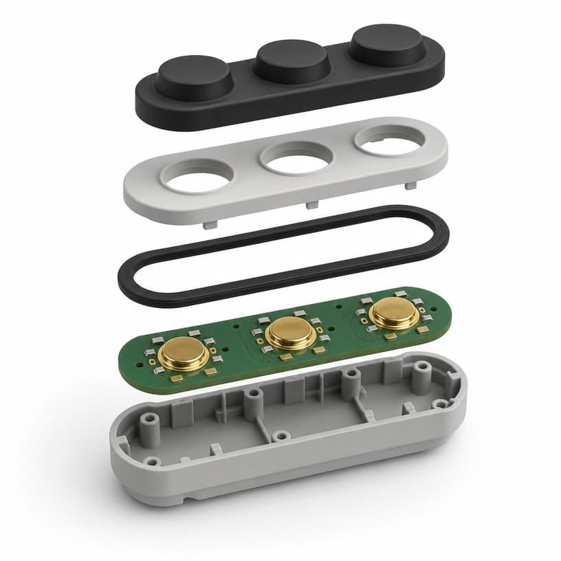
Horizontal Alignment
Vertical Alignment
Contact Area and Electrical Reliability
How PCB Layout Information Should Be Shared for Custom Electronic Level Silicone Keypads
One revision rule that saves money
Using Common Mechanical Datums to Prevent Alignment Errors
Tolerance Management Between PCB, Silicone Keypad, and Housing
Contributor
Typical source of variation
Effect on button travel
Silicone moulding
Shrinkage compensation accuracy, flash, base thickness
Shifts plunger height and contact position
PCB
Board thickness, pad registration, hole position
Moves the contact vertically and horizontally
Injection-moulded housing
Opening size, groove depth, warp across the keypad area
Changes available travel and compression
Assembly
Screw torque sequence, support post contact, keypad seating
Tilts or pre-loads the stack
Environment
Temperature, humidity, compression set over time
Reduces effective travel after release
Why Tolerance Stack-Up Matters
Design Features That Help Prevent Electronic Level Silicone Keypad Misalignment
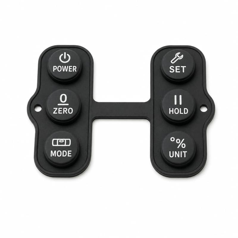
Locating Holes and Positioning Pins
Retaining Ribs and Housing Grooves
Controlled Button Spacing
Flexible Base with Stable Positioning
Prototype Assembly Checks Before Mass Production
Dry Assembly Test
Electrical Function Test
Housing Closure Test
Keep the datum in the loop
Common Mistakes to Avoid When Developing Electronic Level Silicone Keypads
How a Custom Silicone Keypad Manufacturer Can Support PCB Alignment
Electronic Level Silicone Keypad Alignment Checklist
Conclusion
References and Standards Cited
Related reading