How to Turn Design into Reality
- Share
- publisher
- karl
- Issue Time
- Jul 16,2024
Summary
What happens between a partial STEP layout and a buildable silicone keypad design: the four questions that decide structure, how iterations work without new tooling, and what to expect at each step.

A buyer sends a partial STEP layout and a colour preference. Six weeks later there is a moulded keypad in a box. The gap between those two points is silicone keypad design, and it is mostly a sequence of four decisions rather than a drawing exercise.
This article follows that sequence, using the kind of project that arrives without a market sample to copy: a custom keyboard with a PCB, a layout that is only partly defined, and no reference part.
From a Partial Layout to a Silicone Keypad Design
A layout gives key positions and rough key sizes. It does not give the switch principle, the force, the legend method or the panel interface. Those four are what the design phase has to settle, and each one changes the moulding.
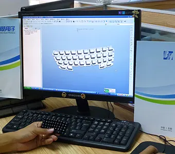
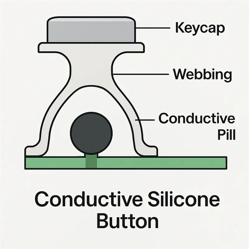
The first task is therefore to establish what the part must do electrically. A carbon pill on PCB tracks, a cavity pressing a membrane switch and a silicone key over a metal dome are three different parts that can look identical from above. The choice drives key height, travel and the underside geometry.
The Four Questions That Convert a Silicone Keypad Design into a Build
Question one: how does the silicone keypad design close the circuit?
Carbon pills are the simplest and cheapest route where the PCB can be laid out to suit. A dome gives a sharper click but adds a component and an assembly step. A membrane beneath the keypad keeps the PCB simple but adds a layer and a tolerance. Once this is fixed, key height and travel follow, which is why it is question one rather than question four.
Question two: what force and travel does the operator need?
This is a design input, not a preference to be discovered at sample stage. A panel used with gloves needs a higher peak and longer travel; a bench instrument used with a fingertip tolerates a short, crisp key. Put a number and a tolerance band on it, and the web geometry becomes an engineering calculation instead of an iteration.
Question three: how is the legend made, and must it be lit?
Moulded relief, printed or laser etched, with or without backlighting. Backlighting changes the substrate, adds coating steps and can add a light barrier, so it has to be decided before the tool drawing. A legend added after tooling is usually printed on top, which is the least durable option.
Question four: how does the keypad seal to the housing?
A flat flange clamped under a bezel, a moulded lip in a groove, or adhesive. Each has a different compression range and a different tool. If the housing already exists, this question is answered by the housing and the design has to fit it; if not, answer it now and design the housing around it.
Iterating a Silicone Keypad Design Without New Tooling
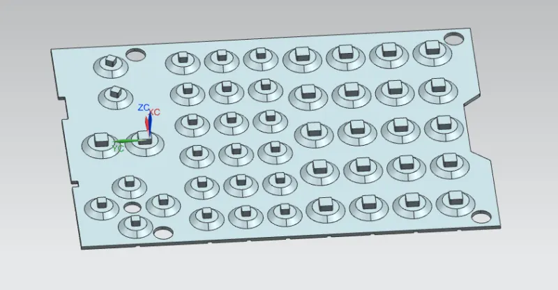
Two structural iterations are normal before sampling. The first usually fixes the interface between the keypad and the PCB: pill height, key height and the space the connector needs. The second fixes the perimeter and the legend, which are the two things a housing change affects.
These iterations are cheap because they happen in CAD. A prototype tool or a machined surrogate then proves the web and the force curve without committing production steel. That sequence is why a project that starts with only a layout can still reach a sample in a few weeks without a tool revision.
What cannot be iterated cheaply is the substrate. Changing hardness changes the whole force curve, so it should be decided with the web rather than after the sample is rejected.
What the Customer Receives at Each Step
| Step | Deliverable | Decision it enables |
|---|---|---|
| Structure review | Marked-up layout with key heights and travel | Approve the switch principle |
| Material proposal | Compound family and hardness with reasoning | Approve the force target |
| Prototype | T0 keypad and force measurement per key | Approve or correct the web |
| Production tool | First-article report and illuminated photographs if backlit | Release to production |
How to Start a Silicone Keypad Design Review
Send the layout, the PCB or its pad drawing, the housing interface, the environment and the number of presses expected. Add a photo of any product the customer considers a good reference, even if it is a different industry. Reference parts communicate force and finish faster than adjectives.
The first return should be a marked-up layout and a short list of decisions, not a price. A price before those four questions are answered is a guess with a number attached. Our guide to conductive silicone button design covers the electrical side in more depth.
A short silicone keypad design checklist
- Switch principle confirmed against the PCB or membrane below.
- Force, travel and overtravel stated with tolerances.
- Legend process and backlight requirement agreed before the tool drawing.
- Perimeter sealing method matched to the housing and its compression range.
- Substrate hardness chosen together with the web, not afterwards.
Can a keypad be designed from photographs alone?
Only for a feasibility opinion. A photograph cannot give key travel, PCB clearance or the sealing interface, and those three decide whether the part can be made at all.
Does changing the colour affect the design?
It affects the process, not the geometry, unless a second colour requires separate keys or a two-shot tool. Backlighting does affect the substrate and coating, so colour and illumination should be decided together.
Silicone keypad design is four decisions in a fixed order: switch principle, force and travel, legend and backlight, sealing interface. Answer them in that order, iterate in CAD, prove the web with a prototype tool, and the production tool will be cut once.