Silicone keypads for smart home device: backlight failure in thin design
- Share
- publisher
- Suey
- Issue Time
- Aug 21,2026
Summary
Miniaturized silicone keypads for smart home devices kills backlight uniformity. Coating variations ruin laser‑etched legends, creating hot spots and illegible symbols. Real cases from Germany and California prove that fixing requires calibrated laser parameters and optical redesign—not generic manufacturing. Without DFM and rapid prototyping, thin designs fail
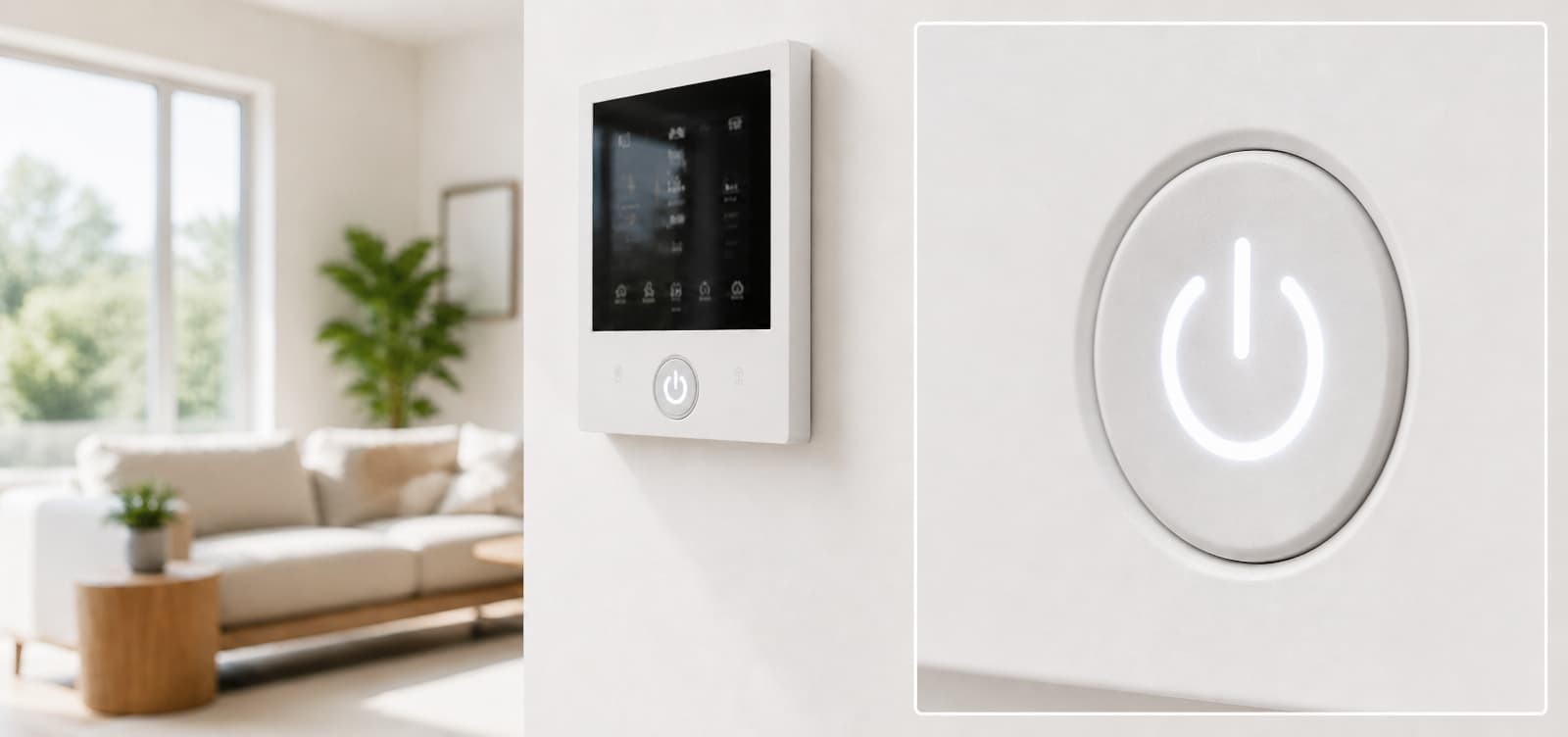
You’ve spent months on the industrial design. The housing is thin, the finish is premium, and the whole look fits your brand perfectly. Then you get the silicone keypad samples – and everything falls apart.
The silicone keypad buttons are too thick to fit the enclosure. Backlight bleeds through adjacent keys. Those tiny icons you designed for the minimalist control panel are illegible in the dark. Worse, after 50,000 presses, the laser‑etched legends start wearing unevenly, and your “premium” device now looks like a cheap prototype.
This is not a rare exception. It happens every day to product teams that treat silicone keypads as an afterthought, rather than an integrated optical‑mechanical system.
The Core Conflict: Miniaturization vs. Backlighting in Silicone Keypads for Smart Home Devices
Smart home devices are getting smaller. Remote controls are thinner. Wall panels sit flush with the surface. Wearable controllers are barely noticeable. Ultra‑thin custom silicone keypads with stroke as low as 0.3mm are becoming the norm. At the same time, consumers demand crisp, evenly lit backlit legends that work in any light condition.
These two requirements – miniaturisation and backlighting – pull in opposite directions. A thicker keypad gives you more room to manage light diffusion and legend depth. A thinner keypad forces you to compress the entire optical stack: translucent silicone base, white ink layer, dark topcoat, laser‑etched symbols, and protective coating – all within a millimetre. Miss the tolerance by just 0.05mm, and you get light leakage, uneven glow, or legends that vanish when the backlight is off.
Engineers call this the “optical stack” problem. And it is the number one reason why custom silicone keypad projects for smart home devices go back to the drawing board.
Why Laser Etching Is the Standard – and Where It Fails
Laser etching is the dominant method for backlit legends on silicone keypads for smart home devices. The process is straightforward:
- Mold a translucent silicone base with high light transmission.
- Apply a white silicone ink layer to reflect LED light back through the legend.
- Spray the final dark topcoat – typically black or charcoal – which becomes the button’s unlit appearance.
- Use a fibre laser to remove the dark topcoat in the shape of each character, exposing the white layer.
- Apply a protective PU or matte coating to resist wear.
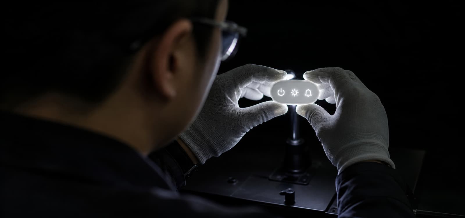
When done right, the legends are invisible when the backlight is off and glow clearly when on. Laser accuracy can reach 0.1mm, and legend positions can be adjusted without new tooling.
But in practice, things often go wrong:
- Inconsistent coating thickness – If the dark layer varies by 0.02mm, the laser may burn through to the silicone in some spots and leave residue in others. Result: ragged edges and uneven brightness.
- Light bleeding – Thin spray coats allow light to escape through the button body. Thick coats alter dimensions and cause assembly issues.
- PU coating rework problems – Once a PU‑coated keypad is laser‑etched, it cannot be reworked. Any defect means scrapping the whole batch.
- Fine symbols – Standard pad printing blurs below 0.3mm line width. Laser can handle it, but only with precise tuning.
Case Study 1: Custom Silicone Keypad for a German Medical Diagnostic Device – Solving the Small‑Symbol Problem
A medical device company in Germany approached us with a tough requirement. Their new handheld diagnostic tool needed a custom silicone keypad with twelve tiny icons – each only 2mm tall, with line widths down to 0.15mm. The design required backlighting, and the symbols had to survive over 200,000 actuations without visible wear.
First attempt – standard pad printing. The ink bled on fine details, and symbols blurred within a few weeks of field testing.
Second attempt – standard laser etching. The symbols were crisp initially, but the laser burned too deep in some areas, causing uneven backlight transmission.
The fix – We used a fibre laser with power and frequency carefully calibrated for that client’s specific silicone formulation and coating stack. We achieved line widths down to 0.1mm. More importantly, we tuned the laser to remove only the topcoat layer without damaging the translucent silicone substrate. The symbols maintained high contrast under backlighting, and the client passed 200,000‑cycle wear tests with no measurable degradation.
Key takeaway – There is no “one‑size‑fits‑all” laser setting. Silicone formulation, pigment load, white layer thickness, and even ambient temperature during etching all affect the final result. Consistent quality across thousands of keypads requires process control that goes far beyond owning a laser machine.
Case Study 2: Silicone Keypad for Smart Home Device – Eliminating the “Hot Spot” for a US‑Based Home Automation Brand
A home automation brand based in California, USA, came to us with a different issue. Their new universal remote control had beautiful backlit silicone buttons – except for one annoying problem. The centre of each legend was significantly brighter than the edges, creating an ugly “hot spot” that made the product look cheap.
The root cause was a classic optical‑stack failure. The translucent silicone base was too clear, so LED light passed straight through without diffusing. The white ink layer was too thin to scatter light uniformly. And the LED placement was too close to the key surface, producing a narrow illumination cone.
We fixed it with a systematic redesign:
- Changed silicone formulation – we specified a slightly less translucent silicone with light‑diffusing additives.
- Optimised white layer thickness – increased the white ink layer by 0.03mm to improve light scattering.
- Laser‑engraved micro‑optical channels – we added 50‑80μm wide channels on the silicone surface to guide light with minimal dispersion.
- Revised LED placement – we adjusted the PCB layout to move LEDs slightly farther from the key surface, allowing light to mix before reaching the legend.
The result was uniform illumination across every legend, with no visible hot spots. The client’s product passed user testing and launched with a premium backlighting experience that matched its high‑end positioning.
What to Look for in a Partner for Custom Silicone Keypads for Smart Home Devices
The success of a silicone keypad project often depends on what happens before the mould is cut. Here are the practical things that matter:
- DFM (Design for Manufacturing) feedback – A partner who provides detailed DFM analysis within 24 hours can catch optical‑stack issues, clearance problems, and tolerance conflicts early.
- Rapid prototyping – Sample moulds delivered in 3‑5 days let you test backlighting, tactile feel, and legend clarity with real silicone before committing to production tooling.
- Process documentation – Consistent results require documented laser power, frequency, scan speed, coating thickness targets, and curing conditions.
- Material expertise – Silicone formulation affects light transmission, actuation force, wear resistance, and chemical compatibility. A knowledgeable partner solves problems generic manufacturers cannot.
- Certifications – ISO9001, ISO14001, and IATF16949 indicate mature quality systems and process control.
A Brief Technical Note
FromRubber is a silicone and plastic OEM manufacturer that has been solving backlighting, miniaturisation, and symbol‑clarity challenges for smart home, medical, and industrial clients for years. We offer laser etching with line widths down to 0.1mm, rapid prototyping in 3‑5 days, and full in‑house tooling. We are certified to ISO9001, ISO14001, and IATF16949.
We do not just manufacture silicone keypads – we help product teams resolve the optical and mechanical issues that stand between a good design and a great product.