Silicone Rubber Button Pads Durable Custom Solutions
- Share
- publisher
- karl
- Issue Time
- Aug 29,2025
Summary
A silicone rubber button pad is one moulding doing four jobs: holding the keys, returning them, closing the circuit and sealing the opening. Why snap comes from the web rather than the compound, and how to specify the conductive path.
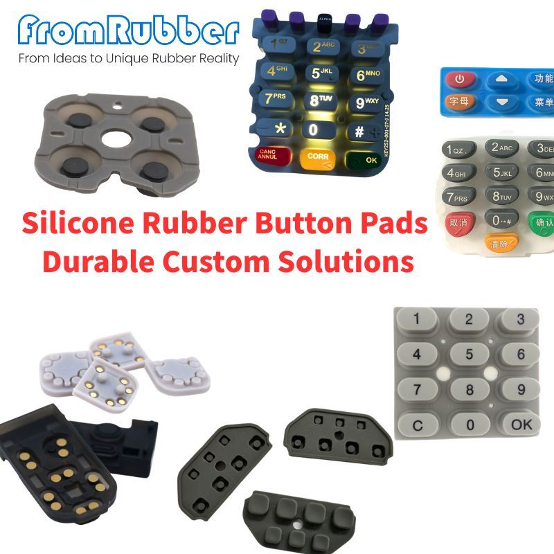
Elastomer keypads / construction - reviewed 11 November 2026
A silicone rubber button pad is one moulded part that does four jobs: it holds the keys, it supplies the return force, it closes the circuit, and it seals the opening it sits in. That is why a pad is specified as a system rather than as a set of button shapes, and why the failure that matters is rarely a broken key.
Most pad programmes come from a device that already exists in a plastic version. The plastic keys work, the buyer wants the same feel in silicone, and the first sample comes back soft. The cause is structural: a silicone key does not click because it is silicone, it clicks because the web behind it collapses in a controlled way.
Definitions. A silicone rubber button pad is a moulded sheet carrying an array of keys, each sitting on a thin web that flexes when pressed. The web is the thin membrane connecting the key to the base mat, and its geometry sets both the actuation force and the return speed. A carbon pill is the conductive pad on the underside of the key that bridges the circuit on the PCB when the key bottoms out.
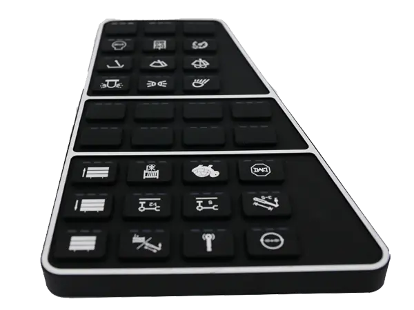
What a silicone rubber button pad actually contains
| Element | What it does | What goes wrong when it is under-designed |
|---|---|---|
| Key top | Carries the legend and takes the finger load | Shiny wear patch, legend loss, or a top that tilts |
| Web | Returns the key and creates the snap | Mushy press, slow return, or a key that stays down |
| Conductive contact | Bridges the PCB pads | Rising resistance, missed presses, drift after months |
| Base mat | Holds the array together and locates it | Pad walks in the housing, keys misalign with the PCB |
| Coating or print | Legend, colour, backlight masking | Ink wear at high-touch edges, uneven lighting |
Snap comes from the web, not from the compound
When the finger pushes a key, the web stretches until it passes a point where it would rather buckle than stretch, and it collapses. That collapse is the click. A stiffer compound makes the collapse sharper but also raises the force; a thinner web lowers the force but slows the return. Because both effects are geometric as much as material, the same 50 Shore A compound can produce a light key or a heavy one depending on the web.
The conductive path is a separate life limit
The circuit does not care how good the click feels. Carbon pills hold a stable resistance but need a flat, clean PCB pad; printed conductive ink is cheaper and thinner but is a wear layer whose resistance climbs with cycles. The number worth specifying is contact resistance at the end of the rated life, measured on the assembled unit rather than on a loose pad.
Sealing, mounting and the housing interface
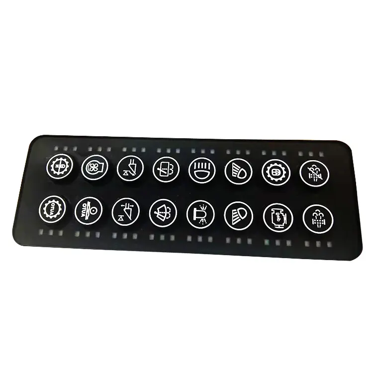
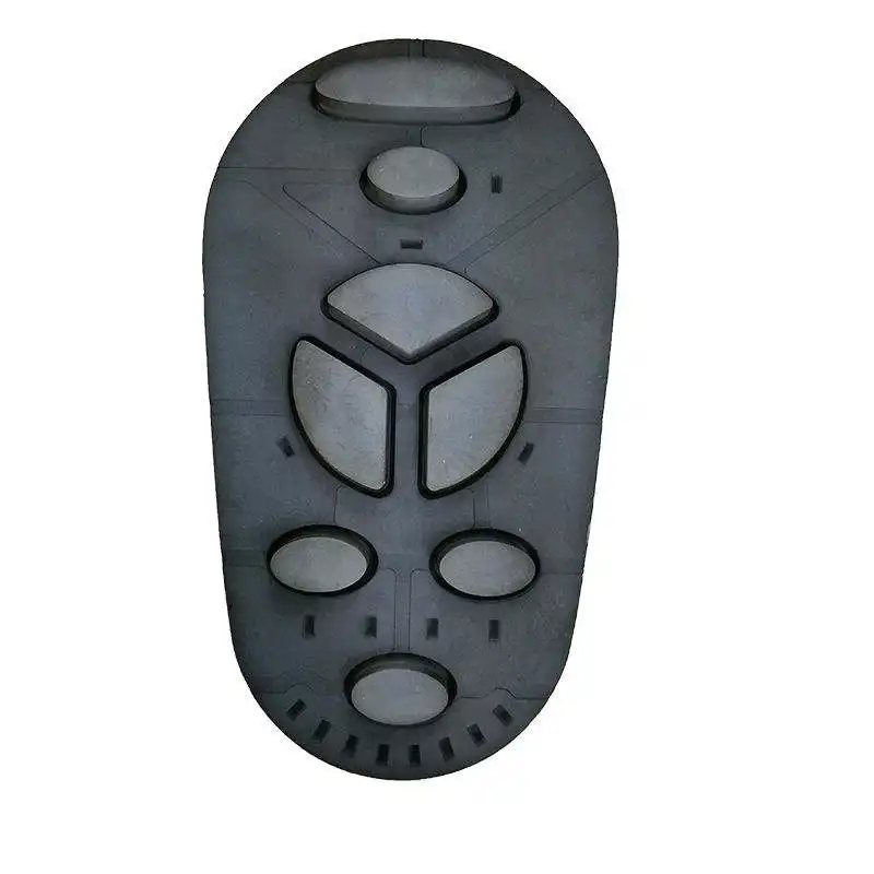
A pad is not sealed by being silicone. It is sealed by how it meets the housing: a moulded perimeter bead compressed by a bezel, an adhesive bond line wide enough to survive thermal cycling, or a clamping frame that keeps the bead loaded. Deciding which of those applies changes the base mat design, and it should be decided before the tool exists.
Location matters as much as sealing. A pad that can shift by a millimetre will put its carbon pills off the PCB pads, and the symptom is not a dead key but an intermittent one that passes final test and fails in the field. Two moulded location pins, or a keyed edge on the base mat, are cheap insurance.
Backlighting without an opening
Light is usually carried through the pad rather than through a hole in the housing. That means translucent silicone in the legend area, an opaque mask everywhere else, and a light guide or diffuser beneath. The design consequence is that the pad becomes two materials in one moulding, which is a tool decision rather than a cosmetic one.
Cleaning is part of the specification
Pads in medical, food and industrial equipment are wiped with alcohol, bleach or solvent. The moulded surface survives those; the printed legend and the adhesive may not. Naming the cleaning agent in the brief turns a vague durability claim into a test that can be run before the tool is cut.
Where a pad earns its place
The same construction appears across five product families, and what changes between them is the environment rather than the mechanism. Reading by environment is more useful than reading by industry, because two customers in different sectors with the same cleaning routine need the same pad.
| Family | Dominant requirement | What it changes |
|---|---|---|
| Consumer electronics | Cost at volume, clean cosmetics | Adhesive backing, printed legends, one moulded colour |
| Automotive | Heat, vibration, UV | Harder compound, moulded legends, location pins |
| Medical | Wipe-down and repeatable force | Sealed perimeter, moulded legends, documented inspection |
| Industrial control | Gloves, oil mist, high cycle count | Higher force, carbon pills, clamped mounting |
| Home appliances | Simple assembly and a flat face | Thin base mat, adhesive, printed graphics |
Material properties that decide how a pad behaves
Tear strength is the web's insurance
A web is a thin section under repeated bending, which is the loading that tears elastomers. Higher tear strength buys tolerance to a slightly sharp root or a thin wall, and it is the property to raise first when a pad fails at the web rather than at the contact.
Compression set is the pad's memory
A pad clamped under a bezel sits under load for years. If the compound takes a permanent set, the key sits lower, travel changes and the snap softens. That is why a pad that measures well when new can feel dead after a summer in a warm enclosure.
Cleaning, service life and the honest end of a pad
A pad is usually replaced as an assembly, not repaired. That makes the service story simple: either the housing lets the pad be lifted and reseated, or the whole front panel becomes the service part. Designing for the first costs a bezel and two location pins; designing for the second means a customer pays for a panel because one key wore out.
Cleaning is the other half of the story. Alcohol wipes attack printed legends long before they attack silicone, and a bleach-based cleaner dulls a matte surface over time. Naming the agent and the frequency in the brief turns a vague durability claim into a test with a cycle count.
Commissioning a custom pad
The fastest route to a working sample is to send the PCB layout with the pad drawing, because the two are one tolerance stack. The silicone keypad manufacturing section covers the tooling route, and the custom silicone rubber keypad page shows the standard construction.
Why does a silicone button feel softer than the plastic one it replaced?
Because the plastic button had a separate spring or a snap dome. In a silicone pad the web is the spring, so the force has to be designed into the moulding rather than inherited from a component.
Can a button pad be repaired?
It can be replaced if the housing allows access. A pad held by a bezel and located by pins is a service part; a bonded pad is not, which is a decision worth taking deliberately.
How many presses should a pad survive?
That number belongs in the specification, because it sets the conductive path. Carbon pills outlast printed ink, and both should be validated at the stated count rather than at first press.
Force, travel and resistance values depend on the pad geometry, the PCB finish and the housing clamp. They should be established on the assembled unit and recorded in a first-article report.
For a button pad programme, send the PCB layout and the key drawing through the quotation file checklist.