Digital Level Silicone Keypad Contact Misalignment: Why Carbon Pills Fail to Match PCB Pads
- Share
- publisher
- FromRubber
- Issue Time
- Sep 17,2026
Summary
Carbon pill to PCB pad misalignment is an interface problem, not a carbon material problem. This article breaks down how a digital level silicone keypad closes a circuit, why pills and pads drift apart during design and assembly, how the tolerance stack-up across keypad, PCB and housing sets the real alignment range, and which inspection and first-article steps catch a marginal contact before tooling is committed.
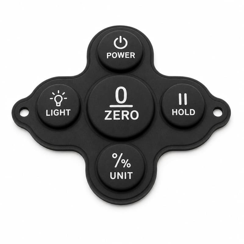
The sample keypad clicked under every finger and the prototype matched the reference instrument. Then the unit went together, the screws were torqued, and ZERO started dropping presses.
Keys that fail only after the enclosure closes are the signature of Digital Level Silicone Keypad Contact Misalignment. Nothing broke a drawing: the keypad, the carbon pill, the board pads, and the housing each sat inside their own tolerance band, and the sum moved the pill off the gap.
Appearance inspection does not catch it: a keypad can pass a visual check while the pill under one button sits 0.25 mm off the pad pattern.
How a Digital Level Silicone Keypad Creates an Electrical Contact
Most keys on an electronic level silicone keypad or an inclinometer silicone keypad are shorting switches. There is no metal dome and no solder joint in the signal path. A silicone button carries a conductive pad underneath, and pressing it against two separated copper regions on the customer's board closes the circuit.
What sits under one button
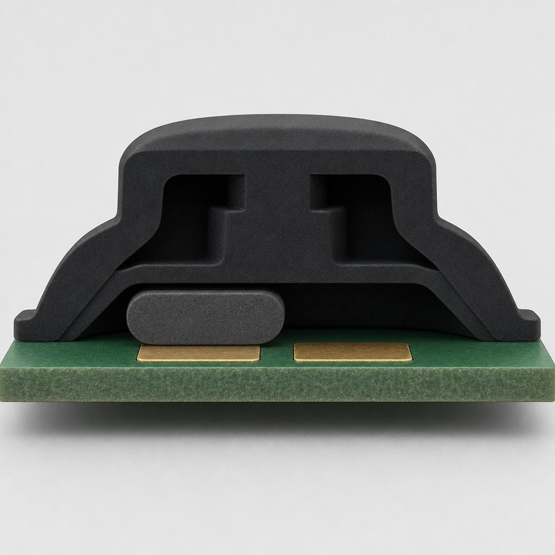
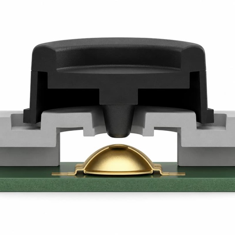
The button top carries the legend, the side wall sets the height, the inclined web is the spring, and the pocket sets how far the conductive element projects below the rubber. A pocket 0.15 mm deeper moves a key from closing at 180 g to 400 g.
The carbon pill has no identity on its own
The pill is a disc of carbon-black-loaded silicone, molded into the pocket rather than glued in. Its resistance on a bench fixture says little, because what matters covers the whole path: pad surface, pill face, pill body, second pad. ASTM B539 covers how static contact resistance is measured, and the reading moves with force and dwell.
Two pads and a gap the pill has to cover
The board pattern is two interdigitated fingers separated by a gap of 0.20 mm to 0.50 mm. The pill does not have to be centered on it; it has to overlap both fingers with margin left over. A 4.0 mm pill on a 5.0 mm pattern leaves 0.5 mm per side at nominal. IPC-7351 covers how that land pattern is dimensioned.
How the contact closes on the bench
Watch the closure under a low power stereo microscope. On a well-aligned pair, contact starts near the middle of the gap and spreads outward both ways; on a misaligned pair it starts on one finger and grows sideways. See carbon pill versus metal dome actuation.
Digital Level Silicone Keypad Contact Misalignment: Where the Mismatch Comes From
Nearly every case follows the same sequence. The keypad drawing is finished first because the housing needs a front panel, the board is laid out later, and nobody overlays them, which is how a silicone keypad PCB mismatch starts.
Two drawings with no shared origin
The keypad is dimensioned from its own outline or locating hole; the board from its own edge or mounting hole. Pick one origin, usually the keypad locating hole and the housing post it sits on, then re-dimension the pill and pad centers from it on a single overlay.
Pads that are too small for the pill
Nominal alignment is what the drawings show; worst-case alignment is what the assembly does. If a pill center can land 0.30 mm from nominal, overlap falls from 0.5 mm to 0.2 mm on the short side and the contact area collapses into a crescent. Bigger pads buy tolerance at the cost of routing space.
The keypad moves while it is being installed
Silicone is elastic. A keypad held only by the front bezel lip can be pushed 0.2 to 0.4 mm sideways while the last corner is worked in, and it will not spring back. Start with why locating holes decide conductive pill position when a unit works on the bench and fails in the housing.
Housing and board referenced from different edges
Four things position the pill relative to the pad: the keypad locating feature, the housing dimension it sits in, the board mounting holes, and the pad position on the board. If the housing is dimensioned from its left wall and the board from its top edge, their tolerances add instead of cancelling.
Check the datum before you check the pill
A pill can be placed correctly in the keypad and still miss the pad, because the datum it was dimensioned from is not the datum the housing locates from.
What an offset pill looks like under magnification
At 20x to 40x, with the keypad held at its installed height, an offset pill shows a lopsided contact footprint: one finger wetted fully, the other only along a crescent. On a gold finish the transfer marks read bright where pressure was high and dull on the far side.
The Tolerance Stack-Up Behind Digital Level Silicone Keypad Contact Misalignment
Treat carbon pill alignment as a sum, not as a property of one part. Four groups contribute: the keypad as molded, the pill position inside it, the customer's board, and the assembly steps.
Keypad molding tolerance
ISO 3302-1 classifies dimensional tolerances for rubber products, and a keypad is specified in one of its classes. The outline is usually stated on a drawing; the key-to-key position taken from a locating feature often is not, and each key's position relative to the others is set by cavity layout and compound flow.
Where the pill sits inside the keypad
During compression molding the pill is placed in the cavity and the compound flows around it. With too little retention it can shift or rotate before the rubber sets, producing pill positions that differ by 0.05 to 0.15 mm inside one tool, so measure pill position per cavity.
What the customer's board brings
Pad location tolerance, plating thickness variation, and mounting hole position arrive with the board. The forgotten number is the reference edge: edges are routed or scored, so a keypad located from a housing post is not comparable with pads dimensioned from an edge.
Assembly adds the last shift
A fastener clearance hole 0.2 mm larger than its screw gives the board 0.2 mm of free travel before clamping, and gasket compression changes the resting height. Settle what a silicone keypad tolerance of plus or minus 0.1 mm really means before the housing drawing is released.
| Contributor | What varies | What it moves | How to read it |
|---|---|---|---|
| Keypad outline | Molding shrinkage | Position in the housing pocket | Compare to the pocket |
| Key-to-key position | Cavity layout and flow | Locating hole to pill center | Optical check, per cavity |
| Pill position in pocket | Retention at mold closure | Lateral shift of the contact face | Cavity spread on the first article |
| Pad location on board | Copper registration | Center of the contact pattern | Measured on a real panel |
| Board edge reference | Routing or scoring tolerance | Anything from the board edge | Re-datum from a mounting hole |
| Fastener clearance | Hole against screw diameter | Board position before clamping | Shift test, loose then torqued |
Worst case, not nominal
Add the contributors arithmetically for a first pass. If the sum already exceeds the overlap you have, no process control on one contributor will rescue the design, because the others can still move to their limit.
Three measurements that predict the stack
Before tooling, three numbers can come off parts you already have: pad-to-pad distance on a real board, key-to-key distance on a molded sample from the intended tool, and the locating hole to the nearest key center on that sample.
Symptoms of Carbon Pill and PCB Contact Misalignment
The signs of carbon pill PCB contact failure follow the geometry, so the pattern usually points at the cause first.
Intermittent response that depends on where you press
A well-aligned key shorts at the center of the gap first, so a light press anywhere on the button closes the circuit. A misaligned key closes only when the pill edge reaches the under-covered finger, so the press point has to be biased. Corner and outer keys, which carry more of the stack, fail first.
Actuation force creeps up
When the pill only partly wets the pattern, resistance stays high until force spreads the contact patch. The user feels a normal click, because the snap comes from web buckling, then presses well past it. A key needing 350 g on a design intended for 180 g has a contact geometry problem.
It works outside the housing and fails inside
A keypad and board tested on a flat bench sit at their nominal separation; bolted into the housing they sit at whatever the tolerance chain produces. When contact tests pass loose and fail assembled, move to board support and keypad location before touching the keypad drawing. Troubleshooting conductive contact failure and carbon pill misalignment sets out that order of checks.
Resistance readings that wander
Contact resistance on a marginal key is unstable rather than uniformly high: 80 ohms on one press, 400 on the next, open on the third. That spread is the signature of an interface made over a crescent instead of a full patch.
Designing the Keypad, PCB, and Housing as One Mechanical System
The work that prevents misalignment happens on paper, before any tool is cut.
Give everything one origin
Nominate the keypad locating hole as the primary datum, its matching housing post as the housing reference, and the board mounting hole that shares that post as the board reference. Then dimension every pill center and pad center from that origin, and overlay the keypad on the land pattern.
Size the pill against the gap, then check the pad
Start with a pill wide enough to overlap both fingers by at least 0.4 mm each at worst case, centered so the overlap is symmetric at nominal. A larger pill is not automatically safer: it adds actuation force and can bridge toward a neighboring pad on a dense pattern.
Add features that stop lateral movement
Locating holes on a spacing that matches the housing posts, a post fit in the 0.05 to 0.10 mm clearance range, anti-rotation tabs, and a bezel lip that traps the keypad edge keep the pill where it was designed to sit. Ribs that only press the keypad down do not stop sideways shift.
Support the board under every key
An unsupported board flexes under press force, and the flex is largest in the middle of a span, often where the center keys are. Housing ribs or support bosses under the key positions remove that variable; press each key mounted and measure deflection at the pad with a dial indicator.
Set the resting height so the pill is not pre-loaded
If the keypad sits in the housing with the pill already touching the pattern, the switch can read closed at rest, or the rubber can take a compression set. There should be a defined gap at rest, and the housing should not squeeze the keypad into that gap.
Design the interface, not the part
The keypad drawing and the land pattern are two halves of one tolerance problem. Reviewed as one drawing from one datum, most contact misalignment is fixed with a dimension change.
Carbon Pill Material and Contact Surface Considerations
Geometry decides whether the pill reaches the pad. The materials decide what happens once it does.
Conductivity is the start of the specification, not the end
A pill specification normally lists a target resistance range measured under a stated force. That number changes with carbon loading, cure state, and pill thickness, and two pills of the same nominal resistance can behave differently because one is softer.
Matching the finish on the customer's board
Gold plated contact surfaces are the usual choice where resistance has to stay low over many cycles, because the surface does not build a thick oxide layer. The mistake is choosing the board finish and the pill specification in two separate conversations. Readings that are high but stable are more often material or surface related, covered in unstable or high resistance on a conductive pill.
Test resistance on the assembly, not on the loose pill
Measuring a pill in a bench fixture confirms the material batch is in range, but not that the key will work, because it skips the web, the pocket depth, the board support, and the pad geometry. Test a molded keypad on a board cut from the production panel, logged key by key. See reading a carbon pill resistance stability report.
Manufacturing Controls That Keep Carbon Pills on Their Pads
Once the design is agreed, the conductive silicone keypad manufacturing controls that hold alignment belong in the purchase specification.
Drawing review before the tool is cut
The review covers the keypad 2D drawing, the customer's contact pad layout, the housing mounting drawing, and the position of every key relative to the locating features. A pill position is only meaningful relative to a datum the housing actually locates from, so reviews at FromRubber are done against the board layout and housing drawing rather than the keypad drawing alone.
Mold design that holds the pill position
The pill pocket has to retain the pill through mold closure. Too little retention lets the pill shift; too tight a pocket can pinch the edge and leave a flash line that reduces the contact face. Multi-cavity tools need cavity-to-cavity consistency checked on the first shots.
Dimensional inspection that includes pill position
Outline dimensions are the easy part. What matters for alignment is the position of each pill center relative to the locating holes, reported per cavity, worst case called out instead of averaged away, with the ISO 3302-1 class named.
Electrical testing that mimics the assembly
Key-by-key switching tests should run with the keypad at its installed height and the board supported the way the housing supports it. A press fixture driving every key at a fixed force and dwell, logging resistance per press, catches marginal keys a hand press misses.
First article validation on the customer's board
The first article should be built with a production keypad and a production panel board, in a production housing when one is available. Every key position gets checked and marginal contact areas are recorded before the design is frozen.
Why a panel photo is not an inspection
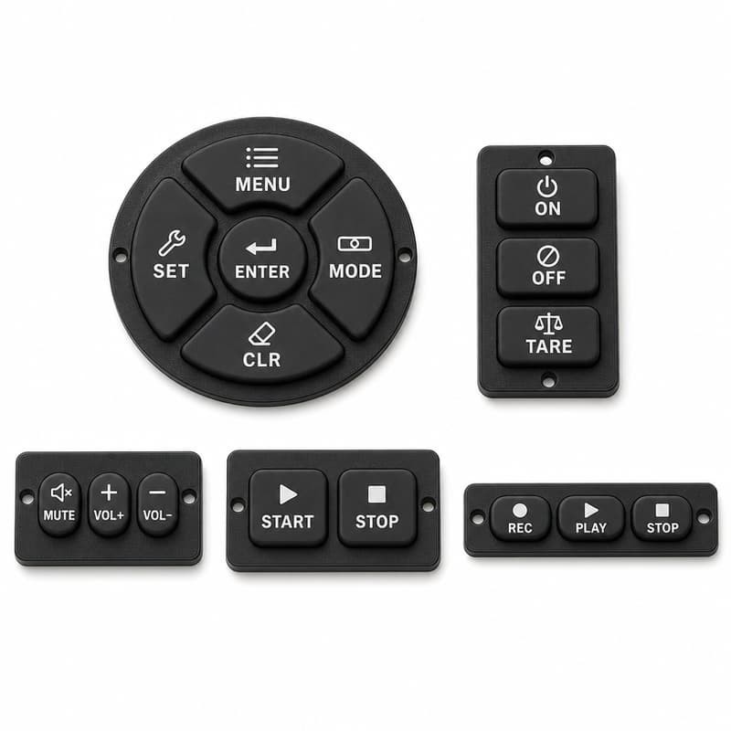
A finished panel shows the legends, the web, and the locating holes, but not where the pill sits inside the pocket, which is the dimension that decides whether the switch closes. Ask for the pill position numbers per cavity and the electrical log from the assembled test.
Digital Level Silicone Keypad Contact Misalignment Troubleshooting Checklist
Work down this list in order. Each row is written so a marginal result is identifiable.
| Check item | What to verify | How it fails |
|---|---|---|
| Pill center against pad center | Overlay both drawings from one datum | A constant offset across units |
| Pad size against pill size | Overlap left on each finger at worst case | Contact along a crescent |
| Keypad locating features | Holes, posts, and anti-rotation tabs engaged | Keys drift while the bezel is fitted |
| Housing fit | Free movement after the bezel is fastened | Bench pass, assembled fail |
| Board support | Rib or boss contact under each key | Board flex, contact needs a heavier press |
| Mold tolerance | Pill position per cavity | A spread inside one tool |
| Assembly testing | Every key logged at installed height | Marginal keys average out |
| Board surface finish | Finish matched to the pill | High but repeatable resistance |
What to Send Before You Order a Custom Digital Level Silicone Keypad
Alignment review needs the board, not only the keypad.
The document set that makes review possible
- Keypad 2D drawing with key centers and locating features.
- 3D model if available, for installed height and travel.
- Board contact pad layout with pad centers from a named datum.
- Housing drawing showing posts, bosses, and bezel seating face.
- Button dimensions, actuation force target, and travel.
- Conductivity requirement with the measured force.
- Operating environment and expected cycle life.
- Legend artwork, colors, and the sealing requirement.
Why a keypad drawing on its own creates problems
A keypad molder cannot verify contact alignment without seeing the pad geometry the pill has to bridge. Every pill dimension then becomes an assumption about a board nobody sent, which is how a part that matches its own drawing still fails in the instrument.
When alignment should be re-checked
Four moments matter. Before mold tooling, on the shared overlay. At first article, with a real board. Before the board goes to volume, in case the panel revision moved a pad. And after any housing change, because a post that moves 0.2 mm re-opens the stack.
Contact failure after assembly
An ordered check sequence for a keypad that passes on the bench and fails once the unit is closed. Read troubleshooting conductive contact failure and carbon pill misalignment.
Holding the pill in position
Why locating holes, post fit, and anti-rotation features decide whether the pill stays on its pad. Read why locating holes decide conductive pill position.
Choosing the switching action
How carbon pill and metal dome mechanisms differ in force, travel, and failure mode. Read carbon pill versus metal dome actuation.
Questions engineers ask after a failed first article
Can a keypad pass appearance inspection and still be misaligned?
Yes, routinely. Appearance inspection sees legends, web condition, flash, and color, but not where the pill sits inside its pocket, because that face points at the board. It is a measured dimension, so ask for it per cavity.
Would bigger pads stop the intermittent keys?
Often, but not for free. Larger pads increase the overlap left at worst case and consume routing space. Compute the overlap remaining on each finger at worst case, then size the pads to leave a margin.
Can this be fixed without cutting a new tool?
Sometimes. A small systematic offset may be corrected by adjusting the pill pockets in the existing cavities, if the change stays inside the available material. A large required shift belongs in the board layout.
Final takeaway
Carbon pill misalignment is almost always an interface problem, not a material problem. A digital level silicone keypad, an electronic level silicone keypad, or an inclinometer silicone keypad has to be designed as one mechanical system with its board pads and housing datums: one origin, geometry sized for worst case, locating features that constrain X and Y, board support under each key, and electrical testing on the assembled unit. Reviewing the keypad drawing together with the customer's board contact layout and housing before tooling carries the most weight, and FromRubber keeps that review inside the same workflow as molding, dimensional inspection, and functional electrical testing of custom silicone keypads for measuring instruments.
Sources and further reading
- Standard Test Method for Measuring Resistance of Electrical Connections (Static Contacts), ASTM B539, https://store.astm.org/standards/b539
- Generic Requirements for Surface Mount Design and Land Pattern Standard, IPC-7351, https://shop.ipc.org/ipc-7351/ipc-7351-standard-only/Revision-b/english
- Rubber, Tolerances for products, Part 1: Dimensional tolerances, ISO 3302-1, https://www.iso.org/standard/62492.html